This edited 2015 contribution to INMR by Eduardo Hilsdorf and the late Manuel Luis Barreira Martinez, respectively from Isoladores Santana, PPC Insulators and the High Voltage Laboratory, Federal University of Itajubá in Brazil offered a comparative evaluation of performance between porcelain line post insulators and polymeric polyethylene pin type insulators applied in covered conductors/spacer cable networks. The research was based on analysis of computer simulation using Comsol Multiphysics® software, visual assessment in specific application conditions by corona camera and the dielectric compatibility test on porcelain insulator and the covered conductors set-ups.
Among the goals of these tests and simulations was to show the possibility of using solid core porcelain line post insulators on compact lines. Another was to challenge the general concept of incompatibility between porcelain insulators and compact network, created in the early years of application of covered conductors when commonly used porcelain pin type insulators (radio-free or not) resulted in punctures to the covered conductor. Values were obtained concerning electric field distribution of these sets that indicated advantages for porcelain line posts in comparison with polymeric pins. Compatibility testing confirmed the possibility of such application.
Introduction
Background & Initial Discussions
In first systems built with covered conductors and operated at 5 kV, acrylic spacers and porcelain pin type insulators were used. Insofar as circuits migrated to higher classes of voltages, new conceptions and models, able to support stresses due to higher voltage gradients were developed. For 15kV voltage class systems this conception was maintained. The only relevant changes occurred in acrylic spacer size and conductor insulation thickness. Field experience, however, indicated components that had been suitably working at 5 kV had no more the same performance level when applied in 15 kV. The increase of the dielectric stresses applied to conductors insulation and the associated high charging currents, resulted in the tracking of the conductors insulation and subsequent erosion of spacers, reducing the system reliability. The first strategy to increase the 15 kV system reliability, was headed to covered conductor improvement.
High Density Polyethylene – HDPE, a material with high molecular weight, was developed aiming to use it in conductors insulation, due to its high dielectric strength and low dielectric constant. Laboratory tests have shown relevant dielectric and mechanical improvements, resulting into higher reliability, when extruded polyethylene in conductor insulation was applied.
In 1960, with the expansion of distribution systems, operation at 25 kV and 35 kV voltage classes became more common, causing RIV (Radio Influence Voltage) problems. To control these problems, the use of RF (Radio-Free) insulators for bare conductor systems had started. Migration to RF insulator application for covered conductor systems was slow and, consequently, immediate problems with conductors for systems equipped with this type of insulator did not occur.
Therefore, in the building of compact network for higher voltages, conceptions and experience coming from 5 and 15 kV projects were used to develop systems with voltage class of 25 and 36.2 kV. In this case the unique relevant evolution was, initially, the changing of conductor insulation thickness. Therefore, spacers for 36.2 kV systems maintained the same insulation distances as for 15 kV.
In the mid 1960s, three-phase measurements of the system charging currents under operation in simulated conditions (salt fog), have indicated tracking resistant polyethylene was, due to its spreading characteristics (dropping, spilling) of water, the material with the best performance also for spacers. During that period, the more usual insulators installed
in 36.2 kV distribution networks were of porcelain solid core post type. In retrospect, it is now known post type insulators were the most suitable for the developing of Spacer Cable systems, due to their low capacitance, as well as the electrical field distribution around themselves. Therefore, no immediate problems occurred with these new materials, tracking resistant.
The majority of failures in compact network involved insulators, usually taking a time to be detected. Experience with many circuits allowed to recognize it was a common failure. The trend to failure in 15 kV systems was accelerated by the replacing of common pin type insulators with radio free pin type insulators, and in the case of 36.2 kV systems, by the replacing of line post porcelain solid core insulator with porcelain pin type single-part insulator Class 55-6 in accordance with ANSI C29.5 Standard. Development of a new insulator with better reliability for Spacer Cable system was necessary. The use of polyethylene for cables and spacers produced positive results that it rendered obvious the use of the same material to develop a suitable insulator, taking to the development of a polymeric post type insulator. In this phase manufacture problems had arisen. The focus was, then, obtaining a polymeric pin type insulator. Consequently, due to the above, mainly as for the application of ceramic pin type insulators, radio-free, a habit was consolidated not to use porcelain insulators in compact networks. This practice spread out and utilities adopted, as a standard, polymeric pin insulator in compact networks.
Motivation
Geometry and materials used in the manufacture of spacers, insulators and fastening accessories, have an influence on the electric field distribution and how the contaminants are trapped.
In operation, compact networks are submitted to several stresses, such as temperature change, electrical field, mechanical stresses and environmental influences. Networks can, therefore, exhibit differences on performance under these many stresses. Single or compound stress action is responsible for ageing and degradation of polymeric materials and can bring the insulated system up to the loss of minimum requirements for operational continuity.
The dielectric withstanding of an insulated surface is essentially reduced when submitted to determined climate conditions, such as rain or high humidity. This reduction can become more outstanding, when the insulated surfaces are exposed to a contaminated atmosphere. A contaminated atmosphere means, from an electrical point of view, a condition that, during a certain period of time, it is easy the development, on the insulated surface, of a layer with substances which dissolved in water, produce conducting solutions. No considerable changes occur, in the dielectric behavior of dry pollution layer and clean surfaces. However, if a moisturizing process takes place, dissolving, but not removing salts partially or totally contained in the layer, electrical arcs can develop on the surface, stirring up a process that can culminate in a disruptive discharge. Furthermore, the developed arcs can generate ozone (oxidant agent), which is one of the responsible agents for the corrosion of insulator fittings.
Polymeric pin type insulators are more and more applied, increasing its share in the market of electrical components, due to their low cost and satisfactory performance in 15 kV systems, built in regions without contamination. In these insulators voids can be present in polymeric structure, caused by air bubbles developed during the polymer injection process. Cracks can also be present, caused by fatigue due to the thermo-mechanical stresses occurred in operation. The electrical field applied and the existence of suitable conditions, such as proper gas pressure inside the voids, can increase the possibility of occurrence of partial discharges inside of the failure zones. The continuous occurrence of partial discharges develops conducting paths in the polymer and usually take material up to dielectric puncture. Damaged insulator can cause line disconnection, and therefore in maintenance costs, together with component replacement as well as an increase of interruption time of electric power supply to customers.
Since there are Brazilian electric power utilities applying Spacer Cables Systems in their overhead networks, equipped with porcelain line post insulators, need is arisen to study and develop a research project, for evaluating the impact of using these insulators in such works.
Technological advance made it possible using numerical methods to calculate electrical fields in complex geometries. Therefore, finite element method modeling were carried out trying to evaluate the impact caused by porcelain insulator application on the voltage gradients in compact network components. Comparative evaluations were also carried out with the use of corona detection cameras and, finally, study hypotheses were validated through the “Dielectric Compatibility Test”, according to parameters of “ABRADEE – CODI-3.2.18.27.1 Standard – Specification of Polymeric Pin Type Insulators for Compact Networks from 13.8 up to 34.5 kV”.
Compact Networks – Field Operation
Natural processes of moisturization, oxidation and contamination of external insulating material can result in the conduction of high amplitude superficial currents.
Current circulation in surfaces with increased conductivity due to the presence of moisture, causes a local heating and water evaporation and consequently a reduction on the surface conductivity, creating dry zones with high temperatures. During the repetition of surface moisturization and drying processes, small arcs occur, short-circuiting dry zones, possibly producing the carbonization of insulating material (tracking) or loss of material (erosion). This phenomenon is, therefore, characterized by the development of carbon by-products, together with bright scintillation, generally called leak current, and produces deterioration of insulating material and tracking development.
Insulating materials for external use, mainly if subject to not uniform electrical fields, must have their capacity for withstanding electrical tracking verified. Another situation that can contribute to or aggravate the occurrence of electrical tracking, concerns dielectric compatibility, when different insulating materials are used together and subject to electrical fields. In these cases, electric field gradients in materials are in inverse proportions with their dielectric constants. Therefore, in a polyethylene (ε1 = 2.3) covered conductor, supported by a porcelain insulator (ε2 = 6) one can expect a gradient of 2.6 times that verified in porcelain, so contributing to establish conditions for an electrical tracking.
This was exactly the condition occurred in the past, on the start of compact network spreading, when pin type porcelain insulators were applied, with a high dielectric constant causing stresses due to the concentration of electrical field in conductor insulation support area and the consequent deterioration in this zone. It is known today this strategy was a mistake which, added to the use of radio free treatment, harmed porcelain insulator image, before any extra study. In opposition to it, this same strategy favored the use of polymeric insulators.
More than dielectric stresses, other factors can influence the superficial ageing of insulating polymers, such as mechanical, thermal and environmental stresses, especially the incidence of ultraviolet radiation. Tracking and erosion phenomena occur in the points of contact of cable with grounded objects, such as tree branches, as well as in the points where cable is tied to insulator groove. Besides, the use of different materials in cables, insulators and accessories several settlements in the same compact network can bring about the occurrence of electrical field concentration and of spatial charge accumulation in interface.
Therefore, the electrical field distribution has an enormous importance when dealing with insulation. If electrical field is very intense in some points of the material, the dielectric strength of this same material can be broken and it passes from dielectric to conductor.
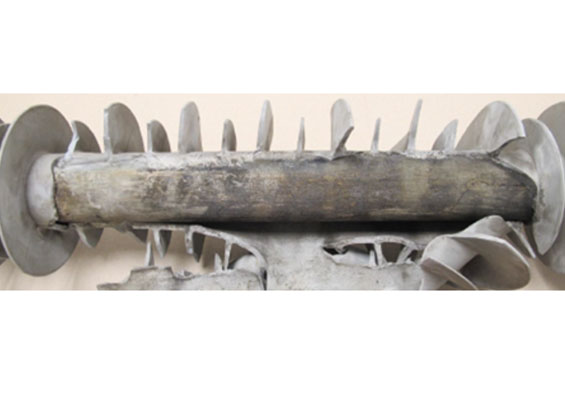
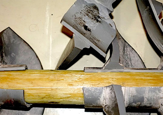
How it can be seen, damages caused by pin type polymeric insulators are several times caused by:
– Partial internal discharge due to the heterogeneity of material used, in the polymeric spacers – Figs. 1 – 3;
– Superficial partial discharge, due to electrical field, exceeding critical value and causing changes on surface, followed by electrical tracking and erosion;
– Cracks caused by sun exposition (ultraviolet rays) and high temperatures coming from manufacturing process;
– Surface contamination of surface due to impurities and the presence of water.
Application of Porcelain to Electrical Insulators
Porcelains are ceramics produced with natural raw materials and used in manufacture of a large variety of products. In ceramics, ionic bonds with a strong covalent character restrict electrons mobility and make them good electrical insulating materials. Therefore, ceramics have a large number of applications in electro-electronics industry, such as, for example, in the manufacturing of electrical insulators.
Technique known as radio free treatment, used for porcelain insulators, is based on the semiconducting glaze on the top and thread of pin type insulator, to keep uniform the electrical field on these two zones, so eliminating the concentration of electrical field inside porcelain. Fig. 4 indicates the radio-free treatment applied to insulators in conformity to ANSI Class 55-6 of C29.5 Standard.
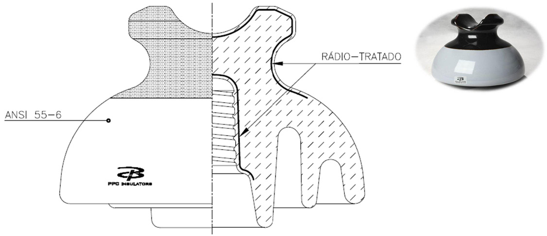
This technique turned out as very efficient for porcelain insulators applied to conventional distribution networks (networks with bare cables), since they drastically reduces the effects of radio-interference and consequently the problems of puncture in pin type insulators, considerably improving the performance of this type of network.
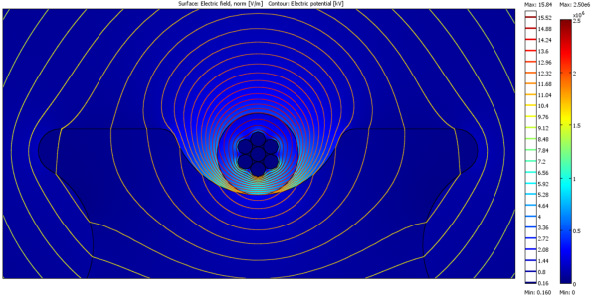
Application of these insulators in compact networks with covered conductors, however, has brought an increase of equipotential line concentration in conductor insulating area, since the reduction of field lines crossing porcelain in radio-free treated insulator caused a concentration in conductor insulation. Fig. 5 shows this effect.
Therefore, in computational simulations and by the assessment of a corona camera, it can be seen the use of this technology worsens considerably the performance of networks using covered conductors (Spacer Cables), because it brings about an electrical field concentration in cable insulation region, causing excessive dielectric stresses.
Experimental Methodology
One of the possible causes for not using porcelain insulators in compact networks would be the dielectric incompatibility of insulator material and cable insulation, taking into account they have very different characteristics.
This factor is not, however, the only one affecting electrical field gradients in the zone of insulator groove. Starting from previous studies, it is easy to observe that the metallic pin of the pin type polymeric insulators brings the ground point of the insulator very near to the phase. Therefore, a concentration of equipotential lines occurs, bringing about an increase of electrical field gradients.
For post type ceramic insulator, ground point is located far away the phase. This type of insulator, however, is manufactured with materials having a dielectric constant higher than the polyethylene of cable insulation.
Therefore, project margins exist to render possible the improvement of covered conductor system and insulator. The one of the objectives of this study is to assess the effect of ground point proximity versus the dielectric incompatibility, initially associated to the difference of dielectric constants.
Evaluations by Assessment of Finite Element- Computational Simulation
Methodology
To identify the critical points of electrical field concentration and to define a comparison criterion between solid core porcelain insulators and pin type polymeric insulators, computational simulations were carried out, using the Comsol Multiphysics® package on several designs of insulators applied to 15 and 25 kV covered conductors networks: pin type polymeric insulators, solid core line post porcelain insulators and solid core line post porcelain insulators with semi-conductor glaze (radio-free). Simulation results are represented by means of a decreasing chromatic scale where red color represents the higher intensity of electrical field.
Considering that the insulator design, as discussed in this paper, was validated by “Dielectric Compatibility Test”, according to parameters of “ABRADEE – CODI-3.2.18.27.1 Standard – Specification of Polymeric Pin Type Insulators for Compact Networks from 13.8kV up to 34.5 kV”, the present modeling were carried out taking into account an applied voltage of 2U0, that is, 16 and 29 kV for systems with 15 kV and 25 kV class voltage respectively.
Generally, field gradients simulations have the objective of determining stress amplitudes and compare them with the critical gradients of the dielectrics, used in dielectric system manufacturing. However, in the present cases the results obtained are also compared for different types of insulators, aiming at observing which of them present the best behavior.
Results
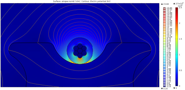
Figs. 6 “a” and “b” shows the modeling results for line post ceramic insulator and pin type polymeric insulator, respectively.
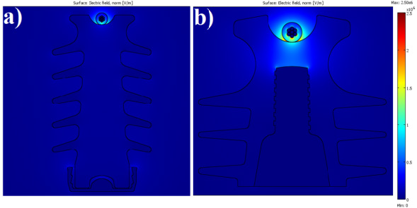
In Fig. 6b electric field concentration is the result of the proximity of grounded pin related to energized conductor. In dielectric terms these stresses are critical mainly for steep impulses. The pin presence also acts in the sense of transferring stresses into cable insulation, as it can be seen through color concentration.
After the demonstration of the feasibility of the application of finite element technique modeling, complementary studies were carried out to verify which of the proposed designs have the potential capacity of satisfying the requests for application to compact networks. To this, the carried out studies evaluate the gradients: E1 – Electric field gradient in the interface between conductor surface and polymer insulating layer & E2 – Electric field gradient in the interface between conductor and insulator support. In these simulations, the covered conductors for 15 kV voltage class were modeled without a semi-conductive layer, recommended in many foreign projects, to get a better uniformity of electric fields.
The electrical field gradients were verified for six different types of insulators, designed to be installed in 15 kV overhead networks with minimum characteristics as follows:
• P1 – Line post ceramic insulator designed for application to 15 kV and 25 kV voltage classes;
• P Study – Line post ceramic insulator with the same height of a 15 kV voltage class line post insulator, but with modified profiles of body and shed to change concentration/dispersion of electrical field;
• P2 – Standard line post ceramic insulator for conventional (bare) networks for 15 kV voltage class systems, used by the majority of power distribution utilities in Brazil;
• P3 – Line post ceramic insulator used by power utilities in Brazil with covered conductors during at least 20 years;
• Polymeric pin type 15kV – High density polyethylene pin type standard insulator for 15kV compact networks, used in Brazil;
• P1-RT (Radio-free) – Line post ceramic insulator, designed for the use in 15kV and 25kV voltage class networks, with the application of semiconducting glaze for radio-interference reduction (RIV).
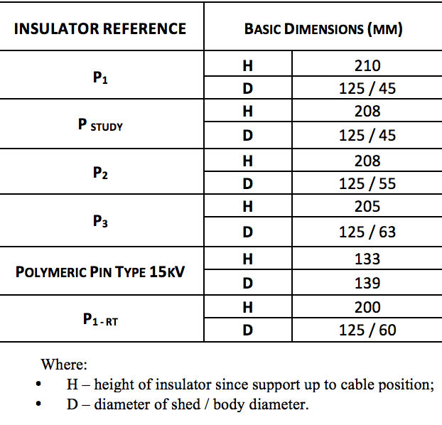
Table 2 exhibits real and percentage comparative results of the simulations. The reference values are obtained for insulators type P1, designed in accordance with Brazilian Technical Standards.
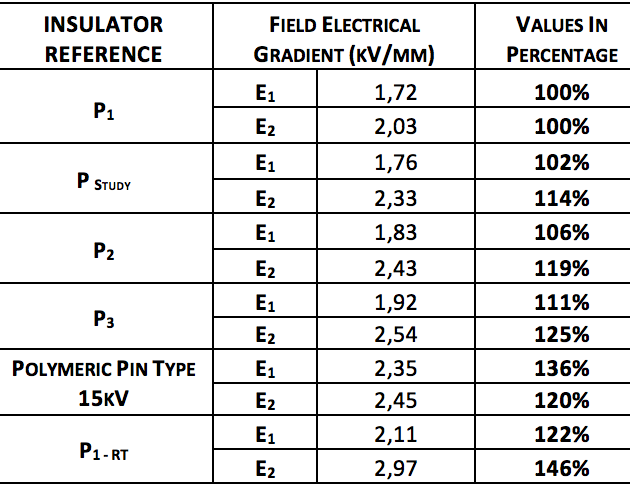
Based on Tables 1 and 2 it is possible to observe:
• P1 insulator, which presents the best performance, has the greatest height and lowest body diameter, if compared to the remaining insulator models, designed for application in 15 kV voltage class networks. Therefore, its efficiency can be attributed to ground plane distance of the energized point and electrical field dispersion along insulator body;
• This same insulator, when treated with semi-conducting glaze in the area of head and groove, P1 – RT, presents the worse dielectric performance, that is, E1= 122% and E2= 146% referred to Project P1;
• Ceramic insulators solid core post type, P2 and P3 references obtained similar performance with little advantage if compared to conventional polymeric pin insulator.
It can be seen that it is possible, with the changing of the ceramic insulators geometry, the height and profile of sheds, to improve the electrical field dispersion in the region of the insulating layer of the covered conductors applied to compact networks.
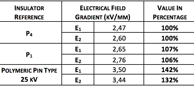
The simulation results shown in Table 2, pointed to the development of the study of a new ceramic insulator design, solid core post type. The results are shown in Table 2 – “P Study” with performance only inferior of the design P1 that was designed to operate also in 25 kV voltage class networks. Therefore, a new set of studies were carried out for a new set of insulators especially designed to application on 25 kV voltage class networks, as shown in Tables 3 and 4, based on P4 insulator. The following projects of insulators were studied:
• P1 – Line post ceramic insulator designed for application to 15 kV and 25 kV voltage classes;
• P4 – Standard line post insulator for conventional (bare) 25kV voltage class voltage networks, used for the majority of the electrical utilities in Brazil;
• Polymeric pin type 25 kV – High density polyethylene pin type standard insulator for 25 kV compact networks, used in Brazil;
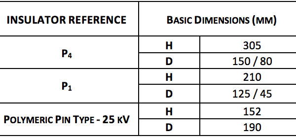
Based on Tables 3 and 4 it is possible to observe:
• Insulator P1, which has the best performance of all the 15 kV voltage class insulators, presents an intermediate performance, due to its lower height compared to the 25 kV conventional insulators;
• P4 ceramic line post solid core insulator presents a higher performance if compared to conventional polymeric 25 kV pin type insulators.
As previously verified, in dealing with the insulator geometry, the ratio between height and profile of the body and sheds, it is possible to improve the distribution of the electrical field on the insulation of the covered conductors.
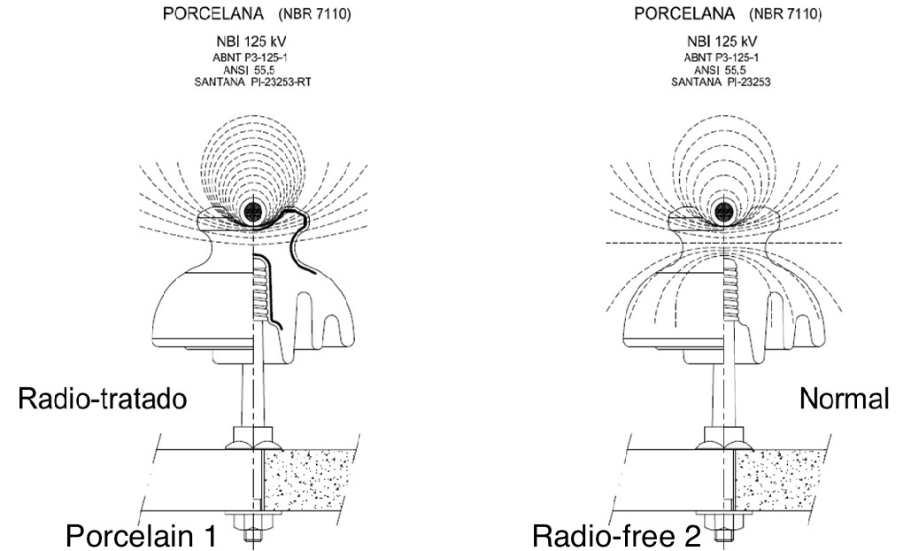
Taking into account that all previous experiences carried out in Brazil condemned the use of radio-free insulators for the application to covered conductors compact networks, the performance of a ceramic radio-free line post insulator was studied. The aim was the analysis of the reasons by which the presence of semi-conductive glaze, applied to the head of radio-free insulators, reduces lifetime of covered conductors. The obtained results can be seen in Figs. 7 and 8.
Observing Fig. 7, in the trial of keeping the potential uniform along all semiconducting glaze, it is obtained a concentration of a greater number of equipotential lines, between cable and insulator groove, resulting in the increase of electrical field gradient.
Finally, comparing the number and shape of the equipotential lines on Figs. 7 and 8, it is noticed that, without the presence of semi-conducting glaze, there is a greater number of field lines crossing porcelain and consequently a lower potential concentration on the region of the insulation of the covered conductor, resulting in a lower dielectric stress. The relation between gradients E2 – Gradient of the electric field in the interface between the external surface of conductor insulating layer and the insulator and E1 – Gradient of electrical field in the interface between conductor surface and the polymer insulating layer of the covered conductor, for both studied insulators, is 1.40 & 1.18 respectively. This indicates, numerically, the heavy concentration of field existing, when radio-free insulators and covered conductors are used.
Analysis of Insulator Performance by Corona Cameras (UV Camera)
Methodology
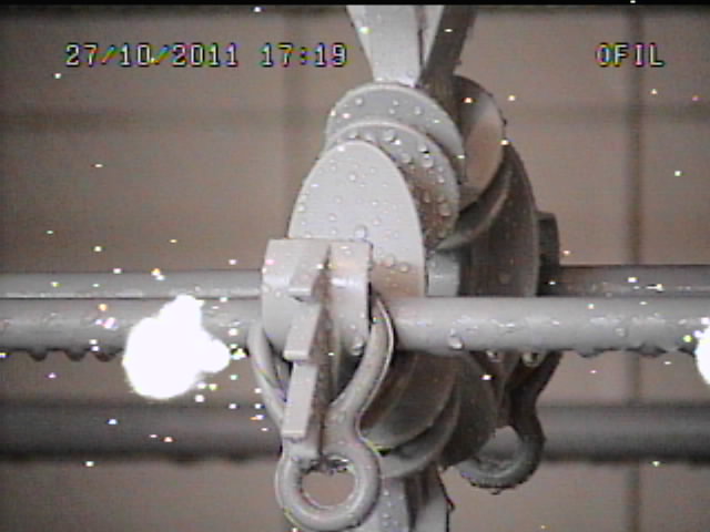
In a laboratory, there are, at least, two methods for inducing external partial discharges on the arrangement made up by covered conductors, spacers and insulators. The first and more common one is dealing with the exposition of the testing set to the condition of rain with standard precipitation rates with conductivity, however, around 750 µS/m. As shown in Fig. 9 this method, used to accelerate the formation mechanisms of external partial discharges, emphasizes problems existing in covered conductors, which are not the object of this discussion, so this test method was not chosen for this verification.
To avoid the influence of conducting rain presence, which can result into a set of fruitless discussions on application validity, insulators designed to for an application on 15 kV voltage class systems, were submitted to dry voltage withstand tests. It is important to emphasize these devices are usually tested always with a voltage equal at least to 2U0, recommended value based on phase to phase system voltage and a safety margin of 15%. During dry test conditions, if a discharge formation process become evident, it is associated to the electric field distribution, without any artificial rain acceleration.
The test set up has an insulator, a covered conductor and a fastening ring. During the energizing of the testing set up with 2U0 the inception of external partial discharges was practically imperceptible. Therefore, to obtain a level of external partial discharges, perceptible by an UV camera, the applied voltage was increased up to 38.5 kV, that is about 5U0 for a 13.8 kV system class voltage. The tested cable, was first supported by a ceramic insulator solid core line post type and, afterwards, by a polymeric insulator. Filming was carried out with a UV camera for all situations and the results were analyzed. In a last situation, it was analyzed the behavior of ceramic pin type insulator, responsible for condemning the use of porcelain in compact networks.
Results
Fig. 10 shows results for the three types of insulator, installed with covered conductor and tied with an elastic ring where, as in Fig. 9, the white dots on the image represent the electrical activity for each case. The analysis of these results is qualitative, through comparison, since methods working with image detection of external partial discharges have not up to now the capacity of associating measured values to operation conditions.
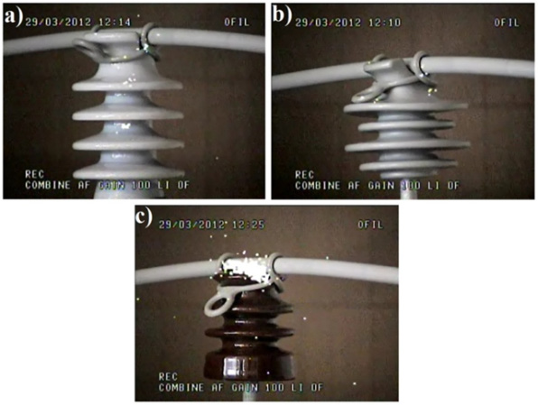
The analysis of the results indicates a strong development of discharges in the interface between the covered conductor and the groove of the pin type ceramic insulator. This is a strong indication that pin type ceramic insulators shall not be used in compact networks, under the risk of causing at medium and long term external partial discharges, capable of compromising the system performance, at best by reducing the dielectric withstanding of the insulators, with the loss of any benefit associated to the better insulating coordination offered by compact systems.
It is also possible to conclude ceramic insulator solid core line post presents a performance similar to that of a pin type polymeric insulator. This makes clear the possibility of using line post insulator jointly with covered conductors and also that the initial application of this technique for covered compact networks, as abandoned due to the problems with the use of pin type ceramic insulators, especially those radio-free type.
Test of Dielectrical Compatibility with Multi-stresses.
Methodology
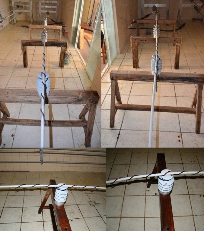
The dielectric compatibility test is carried out in three independent sets. Each set consists of a recommended cable with fastening rings and an insulator or spacer to be evaluated. At least 3 meters of cable per phase and a minimum distance of 1 meter between each set are recommended.
Parameters for test are:
• Temperature on external surface of the cable: 60ºC;
• Rain cycles of 5 minutes aspersion followed by 15 minutes without rain;
• Dispersion: 1 mm/minute;
• Water conductivity: 750 mS/cm;
• Applied voltage: 2U0;
• After thirty continuous testing days, the sets, cable, insulators and spacers shall not exhibit any kind of damage, tracking, perforation or erosion.
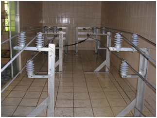
Fig. 11 exhibits the basic diagram of test set up at the LAT-EFEI – Itajubá Laboratory of High Voltage for carrying out the multi-stress compatibility test.
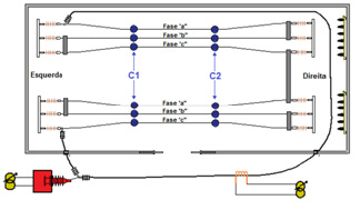
An induction system allows the circulation of current, responsible for keeping cable temperature at 60°C. A voltage source regulates voltage level applied between phase and ground equal to 2U0 with water conductivity constant monitoring. A daily visual inspection and checking of the rain control was carried out, also observing the regulation of the remainder parameters.
Results
Initially, the tests were carried out using covered conductors of national manufacturing, for 15kV voltage class, XLPE manufactured.
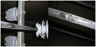
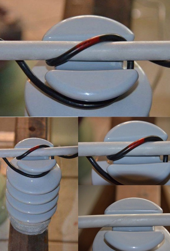
Fig. 12 exhibits photos of test carried out on post type porcelain insulators solid core. It also shows two of the arrangements tested with two cables of different manufacturing, one of gray color at left and the other of black color at right.
This difference of colors represents differences in manufacturing. In this specific case, cable at left was manufactured with two layers, one internal, next to conductor, with semi-conducting characteristics, and the second, external, in standard XLPE framework.
Cable at right was manufactured with a single layer. That allows checking uniformity of electric field internal to cable in test results.
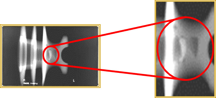
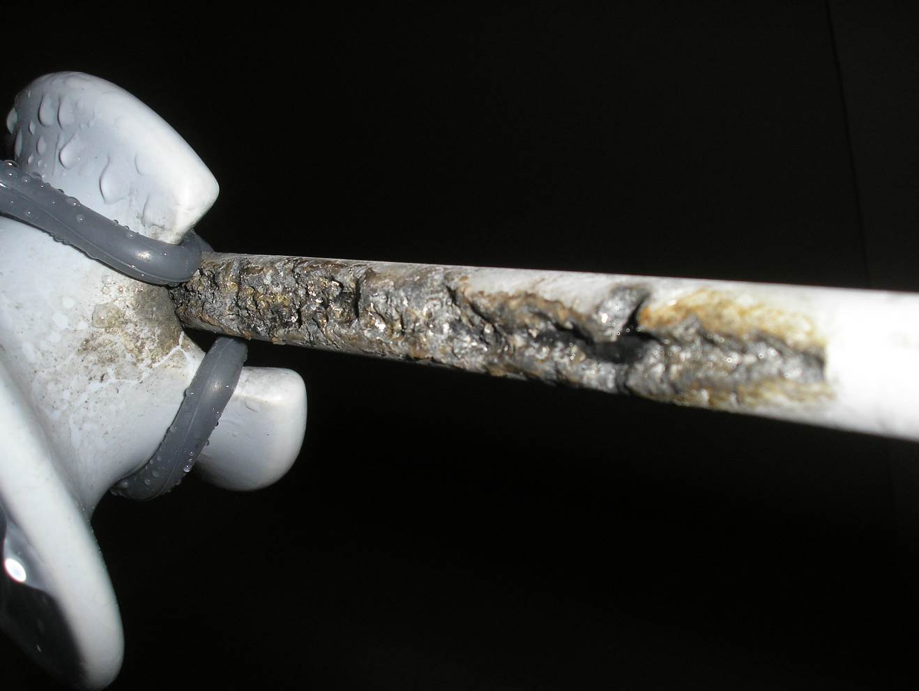
After 5 days of test, for the cable with semi-conducting layer, in accordance with Fig. 13, signals of erosion were already observed at phase “b”, in mid-span, out of simulated critical zone, that is, in the interface zone between cable and insulator. That is an extremely alarming point, because these signals appear in a place not foreseen or explainable through any electrical field simulation.
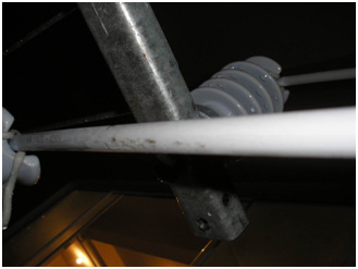
Fig. 14 shows the evolution of problem as noticed, after one day – the 6th. The observed damages are strong indicators that the system has no capacity of withstanding combined stresses of voltage, current and temperature, under the accelerated condition formation of superficial partial discharges, that are responsible for the acceleration mechanisms of natural ageing of the system cable – insulator. This process has a trend to accelerate and take the system to a complete failure.
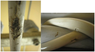
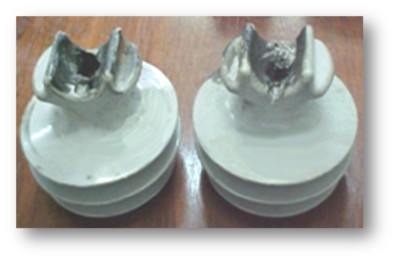
Fig. 15 exhibits results on insulators withdrawn after 10 days of testing, when system can be considered as degraded and in the imminence of failure, in a region out of the insulator groove, what is not expected, indicating a deficiency of cable insulation on those points.
The lack of actuation of protection systems, which can occur in service, because these failures present high impedance, can result in fire ignition, with consequences for patrimony and bystanders. This fact also occurs in laboratory, when the protection of voltage application system is not detuned, as occurred along years of operation of the test system, also used in the development of this work, without any major consequences, for being a system not controlled and without any access.
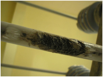
Fig. 16 exhibits the failure evolution “towards insulator”.
Failure starts in a point along the cable. The proximity of a grounded point, in this case provided by insulator (grounded support) makes leak current between energized cable and ground flow through external surface of cable toward insulator.
The superficial conductive carbonized region and tracks developed during this process, sets out towards the insulator groove, that in the end appears damaged and in for someone converted into a possible source of failure, as in the photo. As shown in the photo sequence, however, the insulator was not responsible for the starting of the failure phenomenon, and for that reason, an active role is not attributed to it. This can be also confirmed analyzing Fig. 17, where carbonized dots, in middle-span, are observed far away from insulators. In these cases, the distance from the grounded point, the lack of uniformity of cable insulation and artificial rain, manage to control the current paths towards the grounded points that present higher impedances than those in close zones, reducing the amplitude of superficial current along the cable and, consequently, the observed damages.
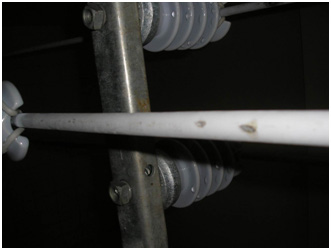
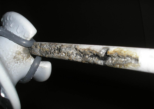
Fig. 18 exhibits results of the tests on the cables of black color, manufactured without the semi-conducting layer next to conductor. In this case a failure is visible in middle – span, related to porcelain insulator and in detail to metallic core of cable.
In short, the defects developed in both types of cable obey to logic as follows, as observed on day + 12:
I – Cables with semi-conductive layer
• PHASE A: Start of erosion.
• PHASE B: Erosion is at 15.5 cm from insulator and with 4.5 cm of extension.
• PHASE C: Start of erosion at 12 cm from the right side of insulator.
II- Cable without semi-conductive layer
• PHASE A: Start of erosion at the left side of insulator groove.
• PHASE B: Erosion on cable at 29.5 cm from the right side of insulator.
• PHASE C: Fastening ring loose.
The Influence of Cable Design and Manufacturing
Since defects have arisen along the cable with semi-conductive layer developing towards insulators and along the entire cable without semi-conductive layer in a random way, the need to investigate this phenomenon was taken into account.
Other types of covered conductors of North American origin exist. In general they are manufactured with three layers, where:
• A semi-conducting layer, independent from the cable class of voltage;
• A layer of low density polyethylene with predominant insulating function;
• An external layer of high density polyethylene HDPE with electro-mechanical function.
In this case, a new test was carried out on 3 sets of 15kV voltage class insulators P2 reference, installed with standard polymeric fastening, to avoid the influence of elastic rings, which presented a high failure/breaking index during previous tests.
A branch of covered conductor of North-American origin was used, duly followed up through daily visual inspection, from September 20th to October 20th with test parameters adjusted as previously described.
During the test and at the test end, no damage, tracking or erosion were observed on interface region between cable and insulators, as can be verified in the images on Figs. 19 and 20. Therefore, the test set up withstood the combined stresses, as claimed by the standards.
Images indicate that no marking was observed on the cables, except salt deposition as a remainder of rain with conductivity corrected to 750 µS/cm, staying with the same appearance at test start.
As can be observed, the design and manufacture of cables used in the dielectric compatibility test have a strong influence on the testing results. In terms of electrical field simulation, points with potential for defects development are the cable to insulator interfaces, what was not observed during the tests and also inspections with UV camera. Analyses presented in the paper “Testing and Analysis on XLPE Brazilian Covered Conductors”, with the authorship of Alan Melo Nóbrega, Manuel Luis Barreira Martinez, Alvaro Antonio Alencar de Queiroz – TDEI, Vol. 20, No. 2, pp. 628-643, 2013, show that: “The data presented in this paper reflect the current status of the quality of commercial XLPE covered cables in Brazil. The results of physicochemical analysis indicated that a low-quality XLPE covered conductors is currently being commercialized in Brazil”.
One can believe these are the reasons responsible for the failures as observed during the tests with cables manufactured in Brazil. These failures do not occur if cables with more elaborate design and manufacturing are used, such as those of North American origin. This paper also indicates the possibility of using porcelain insulators, not radio-free, as shown by the simulations and tests, here discussed, for the construction of compact covered conductors networks once the behavior to the aging tests, as specified by the standards, is determined basically by the cable than by the cable to insulator interface.
Conclusions
The development described above rendered it possible analyzing some potential problems related to polymeric materials used on compact distribution network Spacer – Cable type in Brazil.
Within this context, the case of the dielectric compatibility of the system formed by the ‘insulator – covered conductor surfaces’ was studied in function of the geometry of the dielectrics and their supports and of dielectric constants of the material, taking into account the influence of distance to the ground plane and analyzing its effects through computational simulation, UV camera and dielectric compatibility tests. It was then verified that:
• It is possible to obtain suitable values of electric field gradients for porcelain insulators, solid core post type, calculating them through finite element method, making a comparison with conventional and polymeric pin type insulators;
• With a corona camera, phenomena occurring in the interfaces between insulators and covered conductors were visualized without observing any significant difference in corona level – electrical activity between ceramic insulators post type, and polymeric pin type insulators. On the contrary, for ceramic insulators, pin type, the electric activity level was extremely high, confirming the supposition that its usage is not recommendable in compact networks;
• Through dielectric compatibility test, it was observed that it is possible to use solid core post type insulators in configurations applying covered conductors, especially in compact network systems Spacer – Cable. It is, however, recommended to apply, in these cases, dielectric compatibility tests for the validation of each specific project, since the studies of electric field by finite elements indicate that the insulator design has a relevant influence on the result of electrical field distribution on the system parts involved;
• The behavior of the interface between cables and insulators do not present noteworthy problems, as images emphasizing electric activities in UV field indicate. The same, however, cannot be said as regards to the cables, which are not suitable, even if the insulators – spacers and remaining accessories are developed for this specific application, as indicated by results of tests and suitable studies. Therefore, in this paper it is not considered that the insulators were the inductors of the problems observed on the cables.
It is important to register that, due to cable insulating failures, in regions next to insulators, polymeric pin insulators can exhibit carbonization, transition of phase solid – liquid, or even fire development involving insulator and cable, taking to system interruptions and potential conditions of accidents involving third party: This problem does not occurs in porcelain insulators because, even when the cable loses the insulation, the porcelain insulator is able to maintain system operating, since, on account of the level of dissipated – consumed power during failure process, they do not develop phase transitions and do not come up to flammability condition.
Part of the problem verified, that is the failure aspect and development, is related to the fact that national normalization for covered conductors does not consider the application of the dielectric compatibility test. Therefore a lag exists between the manufacturing of covered conductors and that of their accessories, as demonstrated in this paper, for both porcelain and polymeric materials, as reported. This procedure creates distinct requirements for parts that must operate together, which is a problem for the purchaser, mainly with the ageing of compact networks, because it will be observed only when it will turn into an insoluble problem.
References
1- LOOMS, J. S. T. Insulators for High Voltages. Peter Peregrinus Ltda. England. 1988.
2- MELLO, R.; JÚNIOR, D. C.; BATISTA, T.; MARCONY R.; MELLO, J. Avaliação do grau de poluição em instalações de transmissão, subestações e distribuição. I CITENEL, Congresso de Inovação Tecnológica, Brasília, 2001. (In Portuguese)
3- GODOI, W. C.; SILVA, R. R.; SWINKA FILHO, V.; LODDI, T. Detecção de defeitos em isoladores poliméricos por meio de radiografia digital e reconhecimento de padrões. Espaço Energia, Edição 2, Abril de 2005. (In Portuguese)
4- YOSHIMURA, N.; NISHIDA, M; NOTO, F. Influence of the electrolyte on tracking breakdown of organic insulating materials. IEEE Electrical Insulation Magazine, v. 16, n. 6, p. 510-520, dezembro 1981.
5- FECHINE, J. M.; SANTOS, J. B.; RABELLO, M. S. Avaliação da fotodegradação de poliolefinas através de exposição natural e artificial. Química Nova. vol.29 n. 4 São Paulo July/August 2006. (In Portuguese)
6- MALIK, N. H.; AL-ARAINY, A. A.; QURESHI, M. I. “Electrical in Power Systems”. New York: Marcel Dekker, 1998.
7- TOMIOKA, J. Implementação da Técnica do Pulso Eletroacústico para medidas de perfis de campo elétrico em materiais dielétricos. Tese de Doutorado IFSC/USP, 1999. (In Portuguese)
8-W. M. Carty, J. Am. Ceram. Soc. 81, 1 (1998) 3-20.
9- NÓBREGA, A. M.; MARTINEZ, M. L. B.; QUEIROZ, A. A. A.; Testing and Analysis on XLPE Brazilian Covered – TDEI, Vol. 20, No. 2, pp. 628-643, 2013